

By shrinking the horizontal and vertical dimensions, the electric charge density in various areas (nano-transistor) increases [with the size of the silicon atoms around 46/1 Å (146/0 nm)} _ microelectronics nano Ph.D.
Researcher and author: Dr. ( Afshin Rashid)

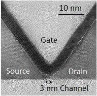
Note: The advent of quantum effects As the transistor shrinks and enters the range below 100 nm, the behavior of individual atoms gradually becomes significant.
Considering the dimensions of the silicon atom, which is about 1.46 angstroms (0.146 nm), and considering the distance between the atomic bonds, we conclude that when we are below the dimensions of 100 nm, with only a few tens of silicon atoms. We are dealing. Decreasing the number of silicon atoms in the transistor makes the problem of crystal defect a serious challenge. Because a small crystal defect, either due to silicon atoms or impure atoms added to silicon, will cause many changes in the electrical behavior of the transistor and take the transistor out of use.
By shrinking all the horizontal and vertical dimensions of the transistor, the electric charge density in the various regions of the nanotransistor increases, or in other words, the number of electrical charges per unit area of the nanotransistor increases. This has two negative consequences : First, by increasing the density of the electric charge, the possibility of discharging the electric charge from the insulated areas of the transistor increases, and this event causes damage to the transistor and its failure. This is similar to the discharge of excess electric charge between the cloud and the ground in the phenomenon of lightning, which ionizes air molecules into negative and positive ions. Second , as the density of the electric charge increases, the electrons may move out of the radius of one atom and into the radius of the adjacent atom under the influence of the momentum or abduction forces that have now increased. This What happens in quantum physics is called tunneling. Electron tunneling from one atom to an adjacent atom is a phenomenon that occurs on a small scale between electrons. This phenomenon is the basis of some electronic components and some nanoscopes. But in nanotransistors, this is not a useful phenomenon, because the tunneling of electrons from one atom to an adjacent atom may continue and cause an electric current. Although this electric current may be very small, because it is unintended and unpredictable, it acts as a leakage path for the electric current and changes the electrical behavior of the nanotransistor.

Conclusion :
Shrinking transistors and entering dimensions below 100 nanometers within the operating range of nanoelectronics technology, although it has many advantages , but faces various challenges.
Researcher and author: Dr. ( Afshin Rashid)
PhD in Nano-Microelectronics